Catalogue Search | MBRL
Search Results Heading
Explore the vast range of titles available.
MBRLSearchResults
-
DisciplineDiscipline
-
Is Peer ReviewedIs Peer Reviewed
-
Series TitleSeries Title
-
Reading LevelReading Level
-
YearFrom:-To:
-
More FiltersMore FiltersContent TypeItem TypeIs Full-Text AvailableSubjectCountry Of PublicationPublisherSourceTarget AudienceDonorLanguagePlace of PublicationContributorsLocation
Done
Filters
Reset
39,458
result(s) for
"Microelectronics."
Sort by:
Modeling and simulation for microelectronic packaging assembly
2011
\"This book is primarily concerned with studies of electronic packaging in assembly manufacture processes and failure mechanisms in assembly manufacture processes and tests through modeling and simulation\"--
From Hydrogenases to Noble Metal–Free Catalytic Nanomaterials for H 2 Production and Uptake
by
Tran, Phong Dinh
,
Métayé, Romain
,
Artero, Vincent
in
Engineering Sciences
,
Micro and nanotechnologies
,
Microelectronics
2009
One drawback of solar and wind power is the need for an efficient storage system to release accumulated energy when neither source is readily available (during still nights, for example). Hydrogen derived from electrolysis of water is potentially a useful medium for this purpose, but catalyzing the interconversion efficiently at large scale would currently require a substantial amount of the scarce precious metal platinum. An alternative approach would be to mimic natural enzymatic reactions, which accomplish the interconversion using hydrogenases that incorporate the more abundant metals iron and nickel. In this vein, Le Goff et al. (p. 1384 ; see the Perspective by Hambourger and Moore ) have lightly modified a hydrogenase-inspired nickel complex in order to append it to a conductive carbon nanotube support. The resulting hybrid material shows promising catalytic efficiency for reversible aqueous electrolysis in a standard apparatus. A nickel electrocatalyst supported on carbon nanotubes shows promising activity for proton-hydrogen interconversion in water. Interconversion of water and hydrogen in unitized regenerative fuel cells is a promising energy storage framework for smoothing out the temporal fluctuations of solar and wind power. However, replacement of presently available platinum catalysts by lower-cost and more abundant materials is a requisite for this technology to become economically viable. Here, we show that the covalent attachment of a nickel bisdiphosphine–based mimic of the active site of hydrogenase enzymes onto multiwalled carbon nanotubes results in a high–surface area cathode material with high catalytic activity under the strongly acidic conditions required in proton exchange membrane technology. Hydrogen evolves from aqueous sulfuric acid solution with very low overvoltages (20 millivolts), and the catalyst exhibits exceptional stability (more than 100,000 turnovers). The same catalyst is also very efficient for hydrogen oxidation in this environment, exhibiting current densities similar to those observed for hydrogenase-based materials.
Journal Article
The future of computing beyond Moore’s Law
2020
Moore’s Law is a techno-economic model that has enabled the information technology industry to double the performance and functionality of digital electronics roughly every 2 years within a fixed cost, power and area. Advances in silicon lithography have enabled this exponential miniaturization of electronics, but, as transistors reach atomic scale and fabrication costs continue to rise, the classical technological driver that has underpinned Moore’s Law for 50 years is failing and is anticipated to flatten by 2025. This article provides an updated view of what a post-exascale system will look like and the challenges ahead, based on our most recent understanding of technology roadmaps. It also discusses the tapering of historical improvements, and how it affects options available to continue scaling of successors to the first exascale machine. Lastly, this article covers the many different opportunities and strategies available to continue computing performance improvements in the absence of historical technology drivers. This article is part of a discussion meeting issue ‘Numerical algorithms for high-performance computational science’.
Journal Article
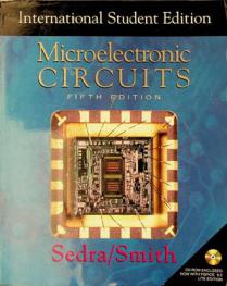
Microelectronic circuits
by
سدرا، عادل، 1943- author
,
Smith, Kenneth C. (Kenneth Carless) author
in
Electronic circuits
,
Integrated circuits
,
Microelectronics
2004
CD-ROM contains: free student version of PSpice 9.2 Lite Edition (SPICE simulator) and new industry-based design examples.
Robust spin crossover and memristance across a single molecule
by
Beaurepaire, Eric
,
Davesne, Vincent
,
Miyamachi, Toshio
in
639/301/119/1001
,
639/925/927/998
,
Chemical Sciences
2012
A nanoscale molecular switch can be used to store information in a single molecule. Although the switching process can be detected electrically in the form of a change in the molecule′s conductance, adding spin functionality to molecular switches is a key concept for realizing molecular spintronic devices. Here we show that iron-based spin-crossover molecules can be individually and reproducibly switched between a combined high-spin, high-conduction state and a low-spin, low-conduction state, provided the individual molecule is decoupled from a metallic substrate by a thin insulating layer. These results represent a step to achieving combined spin and conduction switching functionality on the level of individual molecules.
Switches made up of single molecules form the basis for the concept of molecular electronics. Miyamachi
et al.
demonstrate that an iron-based spin crossover molecule can be switched between different spin states, provided it is decoupled from a metallic substrate by a thin insulating layer.
Journal Article
Planar Slow-Wave Structures
by
Zhao, Chen
,
Aditya, Sheel
2024
This book comprehensively explores the design and application of planar slow-wave structures for millimeter-wave travelling-wave tubes, focusing on enhancing their efficiency and reducing costs. TWTs based on planar SWSs are promising for 5G/6G communications, satellite constellations, automotive radar, and security systems.


