Catalogue Search | MBRL


Are you sure you want to remove the book from the shelf?

{{itemTitle}}
1,028
result(s) for
"Microprocessors Design and construction."
Sort by:

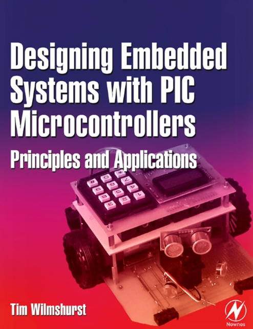
Designing embedded systems with PIC microcontrollers : principles and applications
Embedded Systems with PIC Microcontrollers: Principles and Applications is a hands-on introduction to the principles and practice of embedded system design using the PIC microcontroller. Packed with helpful examples and illustrations, the book provides an in-depth treatment of microcontroller design as well as programming in both assembly language and C, along with advanced topics such as techniques of connectivity and networking and real-time operating systems. In this one book students get all they need to know to be highly proficient at embedded systems design. This text combines embedded systems principles with applications, using the16F84A, 16F873A and the 18F242 PIC microcontrollers. Students learn how to apply the principles using a multitude of sample designs and design ideas, including a robot in the form of an autonomous guide vehicle. Coverage between software and hardware is fully balanced, with full presentation given to microcontroller design and software programming, using both assembler and C. The book is accompanied by a companion website containing copies of all programs and software tools used in the text and a 'student' version of the C compiler. This textbook will be ideal for introductory courses and lab-based courses on embedded systems, microprocessors using the PIC microcontroller, as well as more advanced courses which use the 18F series and teach C programming in an embedded environment. Engineers in industry and informed hobbyists will also find this book a valuable resource when designing and implementing both simple and sophisticated embedded systems using the PIC microcontroller.
eBook
Metamodeling-Driven IP Reuse for SoC Integration and Microprocessor Design
This cutting-edge resource offers you an in-depth understanding of metamodeling approaches for the reuse of intellectual properties (IPs) in the form of reusable design or verification components. The books covers the essential issues associated with fast and effective integration of reusable design components into a system-on-a-chip (SoC) to achieve faster design turn-around time. Moreover, it addresses key factors related to the use of reusable verification IPs for a \"write once, use many times\" verification strategy - another effective approach that can attain a faster product design cycle.
eBook
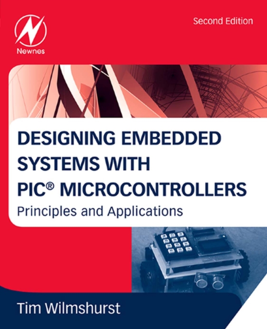
Designing Embedded Systems with PIC® Microcontrollers - Principles and Applications (2nd Edition)
PIC microcontrollers are used worldwide in commercial and industrial devices. The 8-bit PIC which this book focuses on is a versatile work horse that completes many designs. An engineer working with applications that include a microcontroller will no doubt come across the PIC sooner rather than later. It is a must to have a working knowledge of this 8-bit technology. This book takes the novice or intermediate engineer from introduction of embedded systems through to advanced development techniques for utilizing and optimizing the PIC family of microcontrollers in a device. To truly understand the PIC, assembly and C programming language must be understood. The author explains both with sample code and examples, and makes the transition from the former to the latter an easy one. This is a solid building block for future PIC endeavors.
eBook

Modern microprocessor built from complementary carbon nanotube transistors
Electronics is approaching a major paradigm shift because silicon transistor scaling no longer yields historical energy-efficiency benefits, spurring research towards beyond-silicon nanotechnologies. In particular, carbon nanotube field-effect transistor (CNFET)-based digital circuits promise substantial energy-efficiency benefits, but the inability to perfectly control intrinsic nanoscale defects and variability in carbon nanotubes has precluded the realization of very-large-scale integrated systems. Here we overcome these challenges to demonstrate a beyond-silicon microprocessor built entirely from CNFETs. This 16-bit microprocessor is based on the RISC-V instruction set, runs standard 32-bit instructions on 16-bit data and addresses, comprises more than 14,000 complementary metal–oxide–semiconductor CNFETs and is designed and fabricated using industry-standard design flows and processes. We propose a manufacturing methodology for carbon nanotubes, a set of combined processing and design techniques for overcoming nanoscale imperfections at macroscopic scales across full wafer substrates. This work experimentally validates a promising path towards practical beyond-silicon electronic systems.
A 16-bit microprocessor built from over 14,000 carbon nanotube transistors may enable energy efficiency advances in electronics technologies beyond silicon.
Journal Article
Single-chip microprocessor that communicates directly using light
An electronic–photonic microprocessor chip manufactured using a conventional microelectronics foundry process is demonstrated; the chip contains 70 million transistors and 850 photonic components and directly uses light to communicate to other chips.
Chips with everything
The rapid transfer of data between chips in computer systems and data centres has become one of the bottlenecks in modern information processing. One way of increasing speeds is to use optical connections rather than electrical wires and the past decade has seen significant efforts to develop silicon-based nanophotonic approaches to integrate such links within silicon chips, but incompatibility between the manufacturing processes used in electronics and photonics has proved a hindrance. Now Chen Sun
et al.
describe a 'system on a chip' microprocessor that successfully integrates electronics and photonics yet is produced using standard microelectronic chip fabrication techniques. The resulting microprocessor combines 70 million transistors and 850 photonic components and can communicate optically with the outside world. This result promises a way forward for new fast, low-power computing systems architectures.
Data transport across short electrical wires is limited by both bandwidth and power density, which creates a performance bottleneck for semiconductor microchips in modern computer systems—from mobile phones to large-scale data centres. These limitations can be overcome
1
,
2
,
3
by using optical communications based on chip-scale electronic–photonic systems
4
,
5
,
6
,
7
enabled by silicon-based nanophotonic devices
8
. However, combining electronics and photonics on the same chip has proved challenging, owing to microchip manufacturing conflicts between electronics and photonics. Consequently, current electronic–photonic chips
9
,
10
,
11
are limited to niche manufacturing processes and include only a few optical devices alongside simple circuits. Here we report an electronic–photonic system on a single chip integrating over 70 million transistors and 850 photonic components that work together to provide logic, memory, and interconnect functions. This system is a realization of a microprocessor that uses on-chip photonic devices to directly communicate with other chips using light. To integrate electronics and photonics at the scale of a microprocessor chip, we adopt a ‘zero-change’ approach to the integration of photonics. Instead of developing a custom process to enable the fabrication of photonics
12
, which would complicate or eliminate the possibility of integration with state-of-the-art transistors at large scale and at high yield, we design optical devices using a standard microelectronics foundry process that is used for modern microprocessors
13
,
14
,
15
,
16
. This demonstration could represent the beginning of an era of chip-scale electronic–photonic systems with the potential to transform computing system architectures, enabling more powerful computers, from network infrastructure to data centres and supercomputers.
Journal Article
A four-qubit germanium quantum processor
The prospect of building quantum circuits
1
,
2
using advanced semiconductor manufacturing makes quantum dots an attractive platform for quantum information processing
3
,
4
. Extensive studies of various materials have led to demonstrations of two-qubit logic in gallium arsenide
5
, silicon
6
–
12
and germanium
13
. However, interconnecting larger numbers of qubits in semiconductor devices has remained a challenge. Here we demonstrate a four-qubit quantum processor based on hole spins in germanium quantum dots. Furthermore, we define the quantum dots in a two-by-two array and obtain controllable coupling along both directions. Qubit logic is implemented all-electrically and the exchange interaction can be pulsed to freely program one-qubit, two-qubit, three-qubit and four-qubit operations, resulting in a compact and highly connected circuit. We execute a quantum logic circuit that generates a four-qubit Greenberger−Horne−Zeilinger state and we obtain coherent evolution by incorporating dynamical decoupling. These results are a step towards quantum error correction and quantum simulation using quantum dots.
Using germanium quantum dots, a four-qubit processor capable of single-, two-, three-, and four-qubit gates, demonstrated by the creation of four-qubit Greenberger−Horne−Zeilinger states, is the largest yet realized with solid-state electron spins.
Journal Article
CMOS-based cryogenic control of silicon quantum circuits
The most promising quantum algorithms require quantum processors that host millions of quantum bits when targeting practical applications
1
. A key challenge towards large-scale quantum computation is the interconnect complexity. In current solid-state qubit implementations, an important interconnect bottleneck appears between the quantum chip in a dilution refrigerator and the room-temperature electronics. Advanced lithography supports the fabrication of both control electronics and qubits in silicon using technology compatible with complementary metal oxide semiconductors (CMOS)
2
. When the electronics are designed to operate at cryogenic temperatures, they can ultimately be integrated with the qubits on the same die or package, overcoming the ‘wiring bottleneck’
3
–
6
. Here we report a cryogenic CMOS control chip operating at 3 kelvin, which outputs tailored microwave bursts to drive silicon quantum bits cooled to 20 millikelvin. We first benchmark the control chip and find an electrical performance consistent with qubit operations of 99.99 per cent fidelity, assuming ideal qubits. Next, we use it to coherently control actual qubits encoded in the spin of single electrons confined in silicon quantum dots
7
–
9
and find that the cryogenic control chip achieves the same fidelity as commercial instruments at room temperature. Furthermore, we demonstrate the capabilities of the control chip by programming a number of benchmarking protocols, as well as the Deutsch–Josza algorithm
10
, on a two-qubit quantum processor. These results open up the way towards a fully integrated, scalable silicon-based quantum computer.
A cryogenic CMOS control chip operating at 3 K is used to demonstrate coherent control and simple algorithms on silicon qubits operating at 20 mK.
Journal Article
A natively flexible 32-bit Arm microprocessor
Nearly 50 years ago, Intel created the world’s first commercially produced microprocessor—the 4004 (ref.
1
), a modest 4-bit CPU (central processing unit) with 2,300 transistors fabricated using 10 μm process technology in silicon and capable only of simple arithmetic calculations. Since this ground-breaking achievement, there has been continuous technological development with increasing sophistication to the stage where state-of-the-art silicon 64-bit microprocessors now have 30 billion transistors (for example, the AWS Graviton2 (ref.
2
) microprocessor, fabricated using 7 nm process technology). The microprocessor is now so embedded within our culture that it has become a meta-invention—that is, it is a tool that allows other inventions to be realized, most recently enabling the big data analysis needed for a COVID-19 vaccine to be developed in record time. Here we report a 32-bit Arm (a reduced instruction set computing (RISC) architecture) microprocessor developed with metal-oxide thin-film transistor technology on a flexible substrate (which we call the PlasticARM). Separate from the mainstream semiconductor industry, flexible electronics operate within a domain that seamlessly integrates with everyday objects through a combination of ultrathin form factor, conformability, extreme low cost and potential for mass-scale production. PlasticARM pioneers the embedding of billions of low-cost, ultrathin microprocessors into everyday objects.
Flexible electronic platforms would enable the integration of functional electronic circuitry with many everyday objects; here, a low-cost and fully flexible 32-bit microprocessor is produced.
Journal Article

A Compact, Ultra-Wideband, Transformer-Based Quadrature Signal Generation Network in 45 nm CMOS SOI for 5G Applications
In this article, we present an ultra-wideband, fully-differential quadrature signal generation network for 5G applications. The ultra-wideband network is composed of a passive balun and cascaded transformer-based quadrature hybrid. Passive balun converts a single-ended signal to differential with minimum insertion loss, and transformer-based quadrature hybrids are cascaded to suppress I/Q imbalance over an ultra-wide bandwidth. The coupling coefficient of the transformer-based quadrature hybrid is enhanced by adopting vertically stacked multiturn transformer topology to extend operation bandwidth and reduce passive loss and chip area. A novel layout and signal routings are proposed to reduce passive loss, undesired magnetic coupling and I/Q imbalance, making meander lines for phase matching unnecessary. The proposed ultra-wideband quadrature signal generation network is designed in GlobalFoundries 45 nm CMOS SOI process with a core area of 845 μm × 495 μm. The output I/Q magnitude mismatch is less than 0.5 dB from 16 to 60 GHz, and phase mismatch is less than 2° from 16.5 to 54.7 GHz. The input return loss is lower than −10 dB from 22 to 45 GHz, and signal loss varies from 5.74 to 7.4 dB (including 1:2 power splitting and loss from passive balun). The effective image rejection ratio (IRR) is calculated based on I/Q mismatch and is higher than 40 dB from 21.5 to 53.5 GHz.
Journal Article