Catalogue Search | MBRL


Are you sure you want to remove the book from the shelf?

{{itemTitle}}
4,667
result(s) for
"Porous silicon"
Sort by:
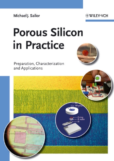
Porous silicon in practice : preparation, characterization and applications
By means of electrochemical treatment, crystalline silicon can be permeated with tiny, nanostructured pores that entirely change the characteristics and properties of the material. One prominent example of this can be seen in the interaction of porous silicon with living cells,
which can be totally unwilling to settle on smooth silicon surfaces but readily adhere to porous silicon, giving rise to great hopes for such
future applications as programmable drug delivery or advanced, braincontrolled prosthetics. Porous silicon research is active in the fields
of sensors, tissue engineering, medical therapeutics and diagnostics, photovoltaics, rechargeable batteries, energetic materials, photonics,
and MEMS (Micro Electro Mechanical Systems). Written by an outstanding, well-recognized expert in the field, this book provides detailed, step-by-step instructions to prepare and characterize the major types of porous silicon. It is intended for those new to the fi eld. Sampling of topics covered: * Principles of Etching Porous Silicon
* Etch Cell Construction and Considerations
* Photonic Crystals, Microcavities, and Bragg Stacks Etched in Silicon
* Preparation of Free-standing Films and Particles of Porous Silicon
* Preparation of Photoluminescent Nanoparticles from Porous Silicon
* Preparation of Silicon Nanowires by Electrochemical Etch of Silicon
* Surface Modifi cation Chemistry and Biochemistry
* Measurement of Optical Properties
* Measurement of Pore Size, Porosity, Thickness, Surface Area The whole is backed by a generous use of color photographs to illustrate the described procedures in detail, plus a bibliography of further
literature pertinent to a wide range of application fi elds. For materials scientists, chemists, physicists, optical physicists, biomaterials
scientists, neurobiologists, bioengineers, and graduate students in those fields, as well as those working in the semiconductor industry.
eBook

Photoluminescence of Structures on Porous Silicon Obtained by Electrochemical Etching with Exposure to Light in Different Spectral Regions
This work focuses on the effect of different additional irradiation sources on the optical properties of porous silicon. Samples were obtained using the standard electrochemical anodization (etching) technique in a hydrofluoric acid solution from monocrystalline silicon wafers. Differences were observed in the photoluminescence spectra of three series of samples subjected to different spectral irradiation. The results show that by using various types of additional light sources during the electrochemical etching process, the photoluminescence spectrum peak of porous silicon can be tuned within the wavelength range of 400–850 nm.
Journal Article

Reflection of Bilateral Porous Silicon with Macropores or Nanowires
The reflection of bilateral porous silicon with macropores or nanowires is calculated according to analytically derived formulas. The formulas take into account the multiple reflections of light at all angles in each porous layer and monocrystalline substrate. Layers of porous silicon are considered as effective media with Lambertian surfaces. The reflection of bilateral macroporous silicon depends on the volume fraction of the pores of the frontal porous layer. The thickness of the frontal layer of macroporous silicon affects the reflection spectrum of bilateral macroporous silicon when the volume fraction of pores is greater than 0.2. The influence of the thickness of the frontal layer of macroporous silicon on the reflectance spectrum of bilateral macroporous silicon increases as the volume fraction of pores increases. The volume fraction of pores of the back porous layer affects the reflection spectrum of bilateral macroporous silicon at wavelengths of light greater than 1.05 m. The volume fraction of pores of the back layer of macroporous silicon affects the reflection spectrum of bilateral macroporous silicon at wavelengths of light greater than 1.05 m.
Journal Article

Porous Silicon Gas Sensors: The Role of the Layer Thickness and the Silicon Conductivity
We studied the influences of the thickness of the porous silicon layer and the conductivity type on the porous silicon sensors response when exposed to ethanol vapor. The response was determined at room temperature (27 ∘C) in darkness using a horizontal aluminum electrode pattern. The results indicated that the intensity of the response can be directly or inversely proportional to the thickness of the porous layer depending on the conductivity type of the semiconductor material. The response of the porous sensors was similar to the metal oxide sensors. The results can be used to appropriately select the conductivity of semiconductor materials and the thickness of the porous layer for the target gas.
Journal Article

Determination of the complex refractive index of free-standing porous silicon and oxidized porous silicon in the Visible and Ultraviolet range
This work determined the spectral values in the 250–850 wavelength regions of the complex refractive index,
n
and
k
, for free-standing porous silicon (PS) and oxidized PS layers. These values were extracted from the experimental reflectance and transmittance spectra. One of the free-standing PS layers was fabricated with high porosity, and the other had low porosity. Thereafter, both layers were oxidized by dry oxidation to achieve a free-standing oxidized PS layer. The oxidation of the porous structures dramatically affects the optical properties of the free-standing layers, especially in the short wavelength Ultraviolet and Visible ranges, since the average transmittance enormously increases, reaching almost 90% at some specific points. Also, we found that the average value of the refractive index and extinction coefficient is higher for PS layers with lower porosity than those with higher porosity. The extinction coefficient and refractive index values are further reduced by oxidizing the free-standing PS layers in the 250–850 wavelength region. The reader can see a zero extinction coefficient value for the oxidized PS layer manufactured with high porosity. Our results show that due to a dry oxidation process in an air environment, the absorption coefficient can be reduced until reaching a value of zero. Due to that, it could be possible to design photonic crystals such as Microcavities, Fibonacci structures, waveguides, and Rugate filters without optical losses caused by light absorption in the Ultraviolet and Visible regions. Pore diameter, thickness and Energy-dispersive X-ray spectroscopy (EDS) elemental spectrum of two different PS layers were determined.
Journal Article
Reflection and Absorption of Two-Layer Porous Silicon
The reflection and absorption of two-layer porous silicon was calculated. Two-layer porous silicon has less reflection than single-layer porous silicon and single-crystal silicon. The reflectance of two-layer porous silicon decreases to a certain value, and then it increases when the volume fraction of the pores of the first layer of porous silicon increases. The volume fraction of the pores of the first layer of porous silicon is greater than the volume fraction of the pores of the second layer of porous silicon. Layers of porous silicon are considered effective media. The lowest reflection of two-layer macroporous silicon is found by optimizing the volume fraction of pores of each layer of porous silicon. The decrease in reflection of two-layer porous silicon compared to the reflection of porous silicon with one layer of macropores is explained. The reflection of two-layer porous silicon exceeds the reflection of single-layer porous silicon and single-crystal silicon when the volume fraction of the pores of the first layer of porous silicon is small and that of the second layer of porous silicon is large. The absorption of two-layer porous silicon with optimized pore volume fractions is 0.88.
Journal Article
Calcium selective optical sensor based on calmodulin functionalized porous silicon
In this work an optical calcium sensor is fabricated using calmodulin surface functionalized macro-porous silicon. Porous silicon is prepared by electro-chemical etching process on silicon wafers, which were further calmodulin surface functionalized for effective calcium binding. Porous silicon provides many fold increase in surface area to volume ratio for absorption, and calmodulin provides effective calcium binding sites. Investigating with different bi-valent and mono-valent cations, the fabricated structure shows effective selectivity and multi-parametric optical response for calcium ions. Several Optical parameters such as reflectance, scattering loss and absorption loss were measured for calcium and other bi-valent and mono-valent cations at physiologically relevant concentrations, the sensor showed great discrimination towards calcium ion. Calcium being the most abundant cation present in the human body plays a significant role in cellular signalling pathways. Moreover Calcium is abundant in drinking water and is important for ecosystem maintenance. The sensor fabricated in this work finds application in calcium sensing in drinking water samples as well as in serum. Thus the sensor provides a highly sensitive, easy to use and cost-effective alternative for calcium detection and sensing.
Journal Article
The influence of the physicochemical processes on the electrical response of Al/p-Si structure with etched surface
In this paper, the electrochemical etching process is used for surface modification of the p-Si wafer, named as porous silicon (PS), in the metal–semiconductor (MS) type Schottky diode (SD) with a structure of Al/p-Si. Five regions of PS wafer with different etching rates are selected for comparison of them which are called P
2
, P
3
, P
4,
and P
5
(P
1
is the reference area without porosity). The morphological, structural, and electrical properties of the PS used in the MS-type SD are investigated using field-emission scanning electron microscope (FE-SEM) images, energy dispersive X-ray (EDX) analysis, and current–voltage (I–V) characteristics, respectively. The FE-SEM images show a meaningful effect on the porosity. The EDX spectrum demonstrates the importance of the chemical effects in addition to the physical changes in the porosity process of the p-Si wafer. The reverse-saturation current (I
0
), ideality factor (n), barrier height at zero-bias (Φ
B0
), and series/shunt electrical resistances are also computed and compared. Some of these parameters (n, Rs, BH) are determined using different methods, namely Thermionic emission (TE), Cheung functions, and modified Norde, and they exhibit strong agreement with each other. The energy-dependent profiles of surface states (Nss) are estimated from the I–V data by considering the voltage dependence of Φ
B
(V) and n(V). All the experimental findings indicate that the etching process of the p-Si wafer significantly influences the electrical performance of the Al/p-Si Schottky diode by increasing the extent of etching.
Journal Article

Green utilization of silicon slime: recovery of Si and synergetic preparation of porous silicon as lithium-ion battery anode materials
With the flourishing development of the photovoltaic industry, the waste of silicon slime generated by photovoltaic cutting has been a serious environmental problem, along with silicon resource waste. In this paper, the waste silicon slime produced by the photovoltaic industry was used as raw materials. Porous silicon particles were synthesized with the magnesium thermal reduction method, combined with hydrofluoric acid etching. The porous silicon can be applied to be the anode material of lithium-ion batteries. The synergistic effect of magnesium thermal reduction and acid etching on the preparation of porous silicon materials was studied. A lower heating rate of 5 °C/min will result in less heat accumulation, which can avoid the formation of large-sized Si/MgO composite particles and obtain a well-dispersed morphology. After a current density of 100 mA·g
−1
, the reversible capacity of porous silicon anode is 751.1 mAh/g after 50 cycles. Compared with commercial nano silicon, its cycle stability and cycle performance have been improved, which provides a new approach for green reutilization of waste silicon slime in the photovoltaic industry.
Journal Article

Progress in Preparation and Properties of Porous Silicon Nitride Ceramics
Porous silicon nitride ceramics is a promising functional ceramic material. In recent years, the research on the preparation of porous silicon nitride ceramics within different methods has been widely investigated. First, this work reviews the main synthesis methods of Si
3
N
4
porous ceramics in detail, and compares the differences between strength and porosity caused by each method. The characteristics and advantages of different technologies under the current conditions were evaluated. Second, the dielectric properties, sound absorption properties and permeability properties of silicon nitride ceramics were compared and summarized based on the experimental results. Third, the applications fields of porous silicon nitride ceramics, such as smelting industry, catalyst carrier, sound absorption, wave-transparent, and biomedical fields were explored. Finally, the assessment of different silicon nitride ceramics preparation technologies was elaborated. This review gives an outlook on the porous silicon nitride ceramics, which shows great potential for further research in this field.
Journal Article